 Extreme Ultraviolet (EUV) Lithography Extreme Ultraviolet Lithography (EUV) is a method of patterning that uses extreme ultraviolet light to produce highly detailed images of surfaces. It has many applications, including manufacturing and designing of semiconductors. However, EUV lithography has limitations, it requires very good contrast, which affects the quality of the patterning. Extreme ultraviolet lithography has become a key technology in semiconductor manufacturing. The technology can print tight pitch metal lines and allow for the mass production of logic chips. In order to achieve cost efficiency and maintain pattern fidelity, the quality of resist used in this lithography process must improve.
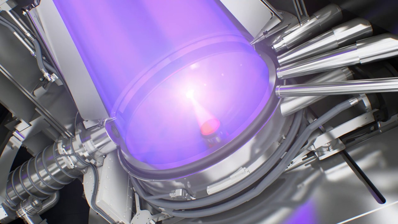
EUV lithography is an advanced fabrication technique that uses light from a 13.5 nanometer laser to create patterns on silicon wafers. This method is used to produce nanometer-scale chips and memory chips. The process is very precise and has the ability to print very fine features on the wafer. However, it also has some limitations. Some of these include the need for a powerful light source and high throughput. The quality of the resulting image depends on several factors, including the process steps and the type of resist used. The global Extreme Ultraviolet (EUV) Lithography Market was valued at US$ 4,660.4 Mn in 2020 and is expected to reach US$ 29,648.4 Mn by 2028 at a CAGR of 26.1% between 2021 and 2028. The best resolution is obtained from cyclic low molecular weight resists, as the protecting number is different in these resists. Another important feature of EUV lithography is that the source should be of the sub-20 nm range. Nevertheless, the power output of the source is limited, so it is essential to have a high-sensitivity resist. High sensitivity resists can help EUV lithography achieve a cost-efficient and scalable industrial application. However, a high-sensitivity resist requires advanced performance characteristics, such as increased material absorption and a superior resolving power. EUV lithography is an emerging technology that allows for the demagnification of mask patterns. Its benefits include lower mask counts and the ability to perform more two-dimensional designs. One potential application for EUV is high-volume manufacturing. Leading-edge memory manufacturers are using it on 10-nm-class DRAM chips. Another possible application is automotive systems, which need to produce data. Both of these applications could benefit from the increased throughput and higher spatial resolution. While a variety of processes are available for this level of lithography, it's likely that the DUV process will remain at the forefront. The key issue is maintaining throughput. This is achieved through new metrology and test capabilities. The future of extreme ultraviolet lithography looks very promising. However, it is still in the early stages of development. Several leading semiconductor manufacturers have invested in EUV, including Intel and TSMC. With the increasing demand for smartphones and other electronic devices, this technology is expected to witness a large demand. However, it is not yet ready for high volume production. There are several limitations that make EUV more difficult to master than most people realize. One of the major limitations is the difficulty in producing EUV light. This is not a suitable process for all applications. However, it is an ideal way to produce tiny transistors on complex chips. Another challenge is the line edge roughness. The EUV resists have a stochastic effect, meaning that lines have uneven edges. Therefore, a high sensitivity resist is necessary to ensure pattern fidelity. Also, to keep cost efficient, the resistance must be able to overcome source brightness issues.
0 Comments
Leave a Reply. |
AuthorWrite something about yourself. No need to be fancy, just an overview. Archives
November 2023
Categories |
 RSS Feed
